- You are here:
- Rave Scientific

- Resources
- Application Notes
Application Notes
What is Raman Spectroscopy?
HOW SCIENTISTS IDENTIFY CHEMICALS USING LIGHT
Microplastics detection in seawater using 2D Raman mapping of a filter (membrane) with residue
INTRODUCTION

Nowadays, microplastics (MPs) – synthetic particles less than 5 mm in size – are widely present in the environment, and seen as a potential global threat to biodiversity, food safety and public health [1]. The problem is especially acute for seawater, since it is one of the main sources of foodstuff, and, at the same time, it accumulates a huge amount of plastic waste. As a result, MPs have already been found in the tissues and organs of many marine species, as well as in sea salt. To control and correct the situation, it is necessary the systematic extensive monitoring of MPs in seawater is including their type/size distribution, spreading over the water area/depth, weathering, degradation, interaction with chemical pollutants etc.
Raman Spectroscopy Quantification of anti-cancer drug via SERS mapping
INTRODUCTION
Therapeutic drug monitoring (TDM) can improve clinical care when using drugs with pharmacokinetic variability and a narrow therapeutic window. Rapid, reliable, and easy-to-use detection methods are required in order to decrease the time of analysis and can also enable TDM in resource-limited settings or even at the bedside. Monitoring methotrexate (MTX), an anticancer drug, is critical since it is needed to follow the drug clearance rate and decide how to administer the rescue drug, leucovorin (LV), in order to avoid toxicity and even death. Quantification of anti-cancer drug via SERS mapping is challenging Raman microscopy applications that typically require research grade systems with deep cooling sensors.
miniRaman spectrometer for cannabis: Part 1. Simple Raman spectra interpretation
PREFACE
The measurements described in this Application Note were carried out in collaboration with Prof. Rime Bahij and Prof. Martin Aage Barsøe Hedegaard from the Department of Green Technology of the University of Southern Denmark (SDU), Odense, Denmark. SDU has a license to cultivate, manufacture, and distribute cannabis, issued by the Danish Medicines Agency in accordance with applicable legislation.
In-vivo skin measurements
INTRODUCTION
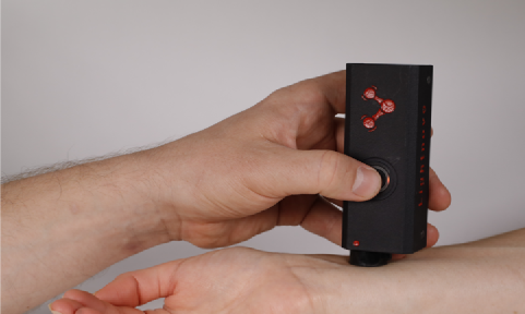
Raman spectroscopy has shown to be a promising technique for different skin diagnostics such as cancer and atopic dermatitis. This technique is non-invasive and can provide several information regarding the molecular composition of the surface of the skin and up to several hundred micrometers in depth.
However in-vivo skin measurements are typically associated with complex Raman instrumentation that requires a deep cooling sensor due to the low Raman cross section of skin, especially at a depth of more than 100µm1,2. Additionally, in-vivo skin measurements require the development of an immersion probe with high numerical aperture NA that can provide a small laser spot size in depth of tissue.
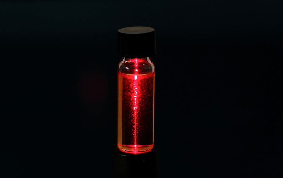
Quantification of toxic methanol in vodka
INTRODUCTION
Methanol is a deadly poison contents in low quality or counterfeit alcoholic drinks. It’s a serious problem can be harmful or even lethal. Poisonings by toxic chemicals as methanol occur all over the world.
In this situation it is advantageous to have a reliable and rapid method for methanol identification and quantification. Raman spectroscopy is a powerful method for material identification that enables rapid, noncontact and non-destructive analysis that can be performed through the glass.
New Technology for Rapid Chemical Characterization of Feedstock Powder
THE CHALLENGE
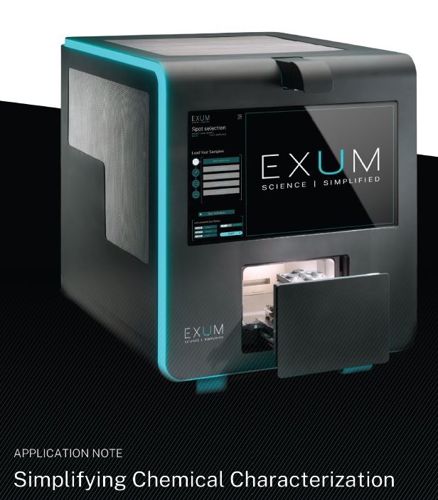
Understanding the chemical composition of any manufactured material is critical to predicting a part’s performance. This is especially important for additive manufacturing because rapidly melting and solidifying materials can affect chemical properties and impact part functionality. Despite its importance, performing chemical characterization is difficult and time-consuming, requiring multiple analytical instruments, complicated operational and calibration procedures, and trained chemists.
Raman spectroscopy of over-the-counter pharmaceuticals and supplements
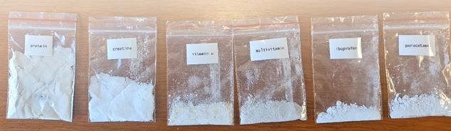
Samples: whey protein, creatine monohydrate, vitamin C, multivitamin, ibuprofen, paracetamol Tools: Lightnovo miniRaman spectrometer equipped with contact probe, Lightnovo Miraspec software.
INTRODUCTION
Raman spectroscopy is a very powerful tool for the analysis and identification of various chemical substances. Raman spectroscopy is widely used in the pharmaceutical industry during analysis of raw materials, quality control, as well as in pharmaceutical R&D. In this application note we are demonstrating the use of Lightnovo’s compact handheld miniRaman spectrometer for the analysis and identification of several different over-the-counter medicines, health supplements such as vitamins, and bodybuilding supplements.
SAMPLES AND SAMPLE PREPARATION
We have chosen the following samples for our experiments: whey protein powder (with vanilla flavour), creatine monohydrate, ibuprofen, paracetamol, vitamin C, multivitamin.
The samples were obtained from the following sources:
- Ordered online on amazon.de (whey protein and creatine monohydrate)
- Purchased in Føtex supermarket in Birkerød, Denmark (vitamin C and multivitamin)
- Purchased in Føtex supermarket pharmacy in Birkerød, Denmark (ibuprofen and paracetamol)
Protein and creatine monohydrate samples were received in powder, and used as received. Vitamin C, multivitamin, ibuprofen and paracetamol were received in tablets. The tablets were crushed into powder with mortar and pestle. The powders were then placed into plastic bags. The samples in plastic bags are shown in Figure 1
Figure 1. The samples used for the measurement.
Lightnovo In-vitro bacteria identification
Introduction
The worldwide increase of antimicrobial resistance (AMR) is a serious threat to human health. To avert the spread of AMR, fast reliable diagnostics tools that facilitate optimal antibiotic stewardship are an unmet need. In this regard, Raman spectroscopy promises rapid label- and culture-free identification and antimicrobial susceptibility testing (AST) in a single step.
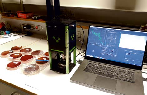
It has been recently shown that multiple bacteria classed can be identified with more than 96% accuracy when machine learning techniques in combination with a novel dataaugmentation algorithm applied.1 Here, we used our miniaturized Raman microscope to measure exactly the same bacteria types as in previous publication, where a research grade Raman microscope with deep cooling CCD was used2 (Figure 1) following identical sample preparation procedures and data analysis (see details in Materials, sample preparation and measurements).
Simplifying Elemental Mapping, from Lithium to Uranium
THE CHALLENGE

As today’s industries strive to improve efficiency and performance while reducing costs, innovative new materials are being tested, developed, and brought to market. From raw material quality control to failure analysis, elemental characterization is a critical part of this lifecycle. Despite its importance, performing elemental characterization is difficult and time-consuming, requiring multiple analytical instruments, complicated operational and calibration procedures, and trained chemists. Traditional mass spectrometry and spectroscopy techniques involve digesting solid material with acid for the most accurate elemental analyses. This results in a bulk composition of the material only and fails to identify how elements change spatially or in depth. Investigating elements’ spatial distributions is especially critical for diagnosing failures in the manufacturing process or after use.
To access spatial elemental data, some users combine mass spectrometry techniques with laser ablation instruments. Due to the complexity of each part of the combined laser ablation and spectroscopy system and lack of continuity between different configurations and vendor combinations, there are still numerous challenges in data collection and processing.
Another approach is to apply scanning electron microscopy with energy dispersive x-ray spectroscopy (SEM-EDX). This can be easier to use than other spectroscopy tools that require liquid sample introduction, but it does not provide high-sensitivity elemental results. SEM-EDX delivers some elemental mapping information, but it can investigate small samples only.
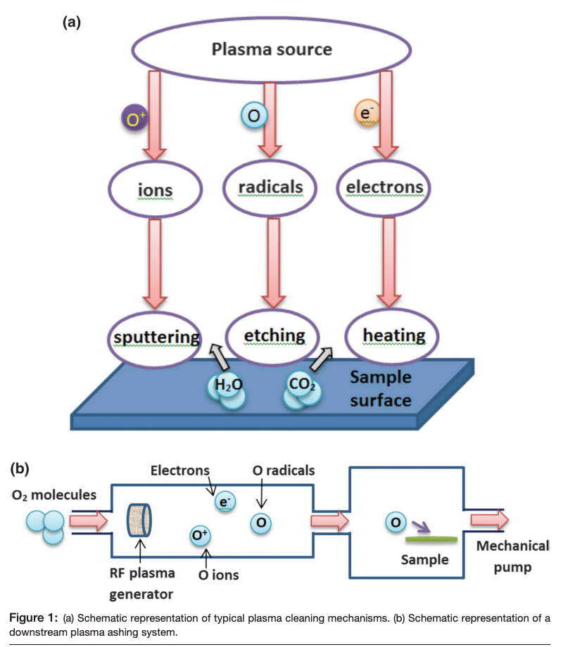
Down Plasma Technology for Cleaning TEM Samples on Carbon Films
Introduction
With the advent of modern scanning/transmission electron microscopy (S/TEM) capable of higher resolution, better contrast,and faster throughput, it is imperative to ensure the cleanliness of the TEM sample under the ultrahigh vacuum conditions of the microscopes [1–5]. It is well known that sample contamination can severely deteriorate the quality of electron microscopy analysis of materials, especially as the sample regions of interest decrease in size. The adverse effects of sample contamination include obscuring the area of the sample being analyzed by buildup of a carbonaceous layer, interfering with focusing and astigmatismcorrection, and generating unexpected microanalysis signals [2, 3].
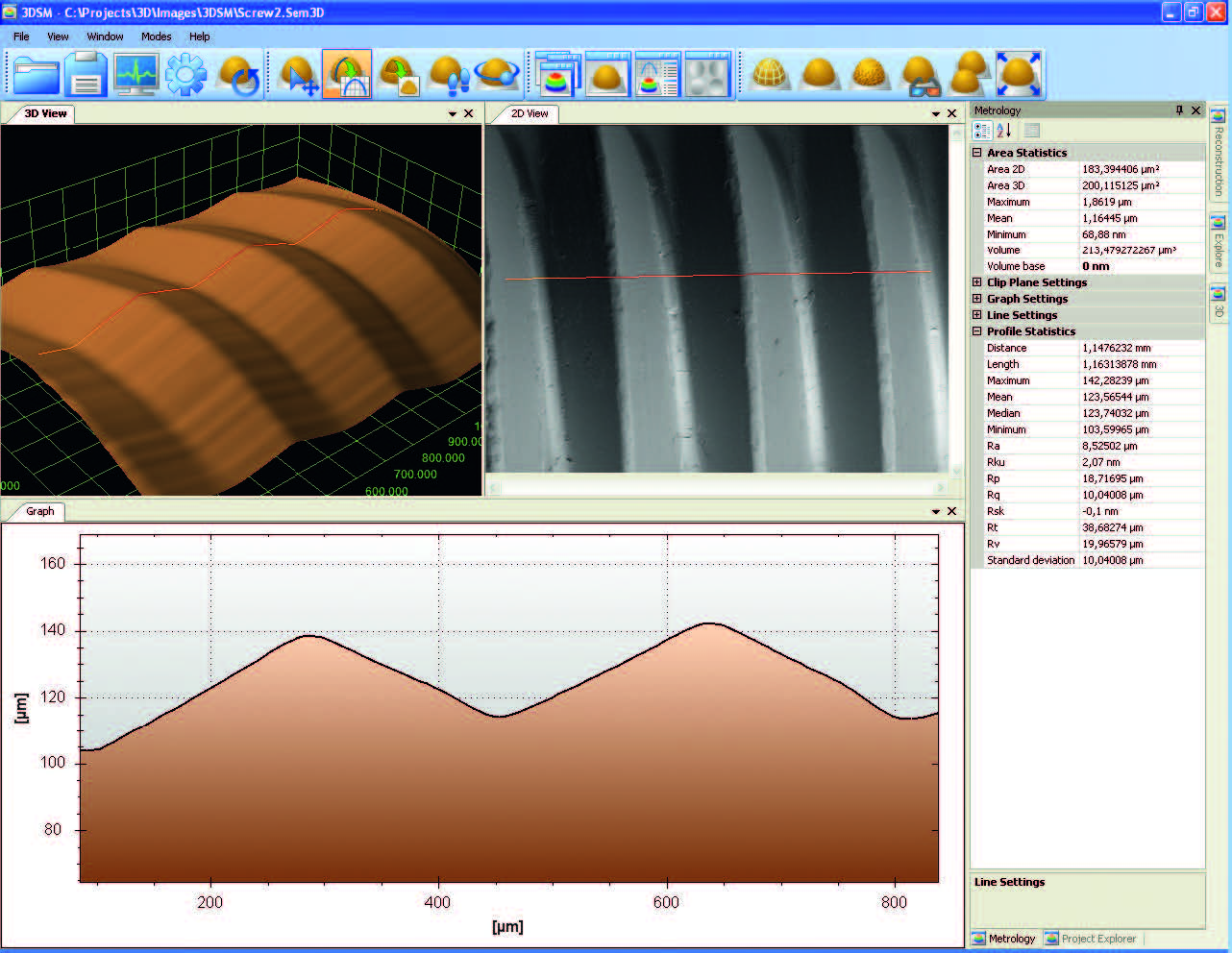
3DSM – 3D Surface Modelling in the SEM
Introduction
What is 3DSM? Scanning electron microscopes are great tools for 2D inspection and metrology of a wide variety of samples. However, their 3D capabilities are still very limited, especially when it comes to quantitative surface characterization. This is the main problem tackled by 3DSM. 3DSM is a PC-based application capable of providing topographical information for samples examined with Carl Zeiss electron microscopes equipped with an AsB® or 4QBSD detector. The application can perform a 3D surface reconstruction based on the individual AsB®/ 4QBSD segment signals, and visualize the resulting 3D model in several different ways. 3DSM can work together with SmartSEM® in the live mode, for real-time 3D imaging. It may also operate in the stand-alone mode for visualizing archived project files.
Ceramics Pre-preparation for FIB-investigation Using ZEISS Crossbeam laser
Introduction
Focused ion beam equipped scanning electron microscopes (FIB-SEM) are widely used in the field of materials science as well as quality control. Not only as a highly sophisticated tool for TEM-sample preparation but also as a versatile instrument for materials characterization. A proven benefit of FIB prepa- ration is location-specific cross-sectioning while maintaining a virtually deformation-free microstructure.

Simple Ways of Reducing Vibration in your SEM Image
Introduction
When imaging in your SEM do you ever experience jagged lines on the edge of your image at high magnification?
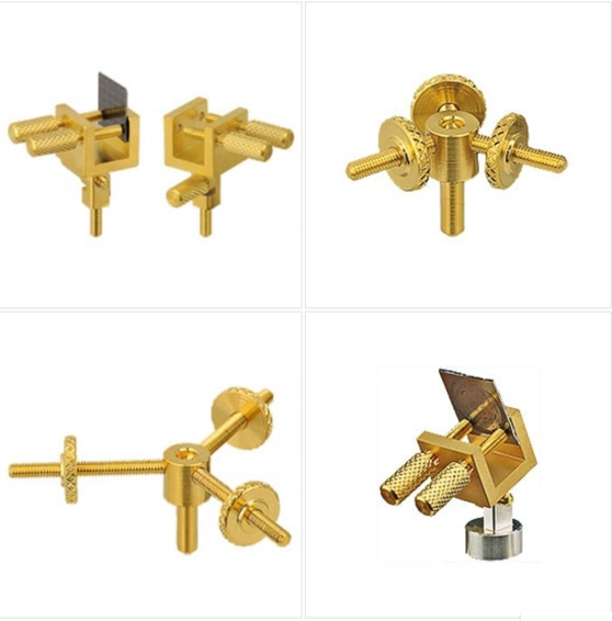
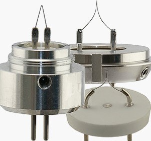
Advantages of Brass Gold-Plated SEM Holders
There are a number of advantages with Brass constructed SEM holders that are coated with gold.
Plasma Processing in the SEM:The Reality (or nuisance) of SEM Hydrocarbon Contamination
Have you ever de-magnified when imaging in your electron microscope and notice dark scanlines on your sample?
Descriptions of Electron Microscope Cathodes and Emitters
The Scanning Electron Microscope (SEM) requires a source of electrons to form a beam and can utilize various emitters.
Proper Target Material Selection when Coating Samples Using an SEM Sputter Coater
In this article, we will identify target material options for use in your specimen coater when analyzing a non-conductive sample.

Removing Cured Epoxy
Epoxies have a wide range of applications in microscopy sample preparation and vacuum chamber feedthroughs or leak repairs.
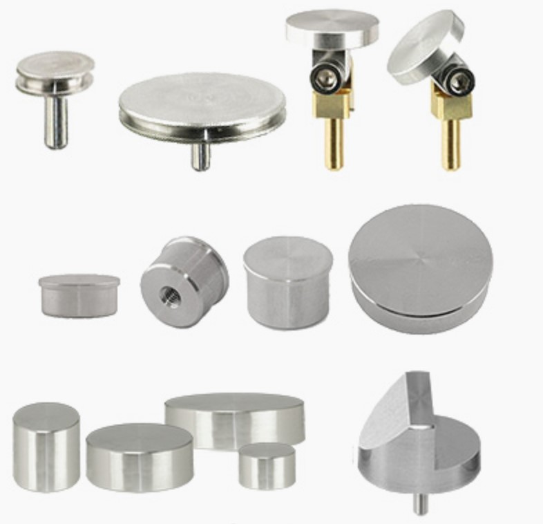
Best Practices for Cleaning SEM Stubs and Mounts
Standard SEM stubs and mounts are used as substrates to mount samples for Scanning Electron Microscopy (SEM).
Optimizing the usage of SEM Sputter Targets
In an SEM sputter coater for coating non-conductive SEM samples, a plasma is created at a vacuum level of around 2x10⁻¹ to 2x10⁻² mbar by applying a high voltage between the grounded sample stage and the target.
Calibrating a Scanning Electron Microscope (SEM)
Although modern manufacturing techniques have greatly improved the accuracy of SEMs, it is good practice to regularly check if the magnification shown on the SEM is still correct.