Ceramics Pre-preparation for FIB-investigation Using ZEISS Crossbeam laser
Introduction
Focused ion beam equipped scanning electron microscopes (FIB-SEM) are widely used in the field of materials science as well as quality control. Not only as a highly sophisticated tool for TEM-sample preparation but also as a versatile instrument for materials characterization. A proven benefit of FIB prepa- ration is location-specific cross-sectioning while maintaining a virtually deformation-free microstructure.
With typical FIB beam diameters ranging from about 5 nm to several micrometers, these systems are primarily used to section regions of a few tens of microns. It is still possible to prepare larger cross- sections that extend to several hundred micrometers in length and depth, but this has shown to be a time intensive method.
To bridge the gap between small-scale FIB preparation and large-scale mechanical sample preparation by grinding and polishing, and to avoid issues with altered microstructure caused by large heat affected ones when using nanosecond or even continuous wave lasers, ZEISS Crossbeam has been equipped with a femtosecond (fs) laser system. The use of a femtosecond laser facilitates extremely fast sample machining and surface preparation of deeply buried features as well as large areas. Additionally, due to the pseudo athermal ablation process, the surface quality often reveals the true microstructure directly on the laser cut cross-section without further (FIB) polishing.
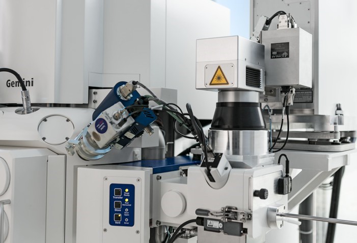
As shown in figure 1 the fs-laser is installed on a separate airlock-chamber and is therefore separated from the SEM main chamber which, with respect to ablating large quantities of different materials, provides huge advantages regarding cleanliness of the chamber and maintenance intervals.
The fs-laser has already been tested on metals and alloys revealing the microstructure and showing that even EBSD measurements are possible directly on the laser cut [1].For e.g. microelectronic components it allows to access deeply buried features for further FIB polishing and analyses [2]. The present work extends the material range addressable by the fs-laser to various technical ceramics, gives milling rates and provides a kind of universal recipe as guideline for machining other ceramics.
Experimental Setup, Results and Discussion
Laser milling experiments were conducted on five different technical ceramics to cover a wide range of materials. Flat samples of Zirconia (ZrO2), Silicon Nitride (Si3N4), Forsterite (Mg2[SiO4]), Lead Zirconate Titanate (Pb[ZrxTi1−x]O3 (0 ≤ x ≤ 1)) and a compound of SiC-ZrB2 were used, all featuring ground surfaces. When approaching a new sample material, the first step... (Read the rest of this article)