- You are here:
- Rave Scientific

- Sample Preparation
- Supports and Substrates
- Silicon Wafers and Chips
Overview
Polished silicon is an excellent substrate for imaging, experiments, nanotechnology and micro-fabrication applications. It is available in the form of wafers, diced wafer or as smaller chips (pieces). The silicon wafer and chips all have a orientation. Cleaving of the wafers to the desired size with a orientation wafers is straight forward and simple. The silicon wafers and chips are all P-type, doped with B to provide excellent conductivity for SEM, FIB and STM applications.
For biological applications silicon resembles glass, which makes it a suitable support for growing and/or mounting cells. For imaging applications, it is an ideal sample substrate for small particles due to the low background signal of the highly polished surface.
Two grades of silicon substrates are offered:
Micro-Tec standard silicon wafers and silicon chips for standard application and medium resolution imaging.
Nano-Tec ultra-flat silicon wafers and ultra-flat silicon chips for demanding applications and high resolution imaging.
Micro-Tec <P/100> standard silicon wafers and diced wafer for SEM substrates
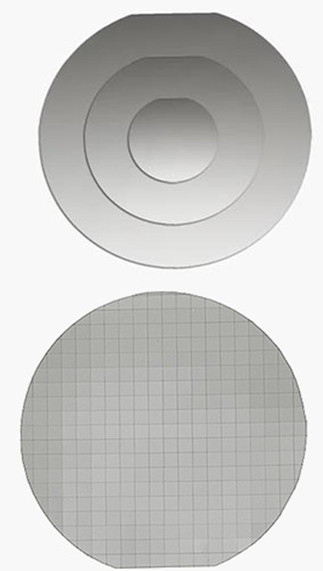
The Micro-Tec <P/100> silicon wafer substrates can be used for sample substrates, micro-fabrication, substrate for thin film research or biological substrates. Useful flat substrate for SEM imaging of particles due to the low background. For biological applications, Si has similar properties as glass and can be used to mount or grow cells. Can be easily cleaved or used as a whole wafer. The Micro-Tec Si wafers are packed in a wafer carrier tray sfor protection. The diced wafer supplied on wafer adhesive disc and packed between two plastic sheets for protection. The Si chips can be easily lift off the adhesive sheet.
The Micro-Tec standard silicon wafer substrates are available as:


