ZEISS GeminiSEM Family
Overview
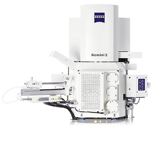
Since the introduction of the ZEISS GEMINI column design in 1994, ZEISS continues to set the standard for Low Kev performance and ease of use. The GeminiSEM delivers effortless imaging with sub-nanometer resolution and high detection efficiency. You can rely on its surface sensitive analysis and profit from the highest sample flexibility. GeminiSEM 560 comes with a novel design of the Gemini 3 electron optics to deliver all-round better resolution, especially at low voltage.
GeminiSEM 460 with its Gemini 2 double condenser guarantees flexibility and ease-of-use, combined with reliable, excellent imaging and analytics. GeminiSEM 360 delivers in surface sensitive imaging so you will experience high contrast, high resolution and extremely large fields of view. Choose these flexible and reliable field emission SEMs for your research, industrial lab, imaging facility or educational organization. With the GeminiSEM family you will always get excellent images and reliable analyses from any real-world sample.The GEMINI FESEM meets the highest demands in imaging and analytics from any sample. The effortless imaging and sub-nanometer resolution of the GeminiSEM is complimented by its best in class detection efficiency, even in variable pressure mode. With the GeminiSEM family you will always get excellent images and reliable analyses from any real-world sample.
Unique Features
- GeminiSEM 560 brings you more signal and more detail, especially at very low voltages. Its variable pressure mode makes you feel like you’re working in high vacuum.
- GeminiSEM 460 is your specialist for speed and surface sensitivity. Profit from ease-of-use by design and flexibility for imaging and analytics.
- GeminiSEM 360 lets you experience high resolution and high contrast even on extremely large fields of view. Especially, but not solely, liked by novice users at high or low vacuum.
Your Insight into the Technology Behind It
Capitalize on Gemini Optical Design
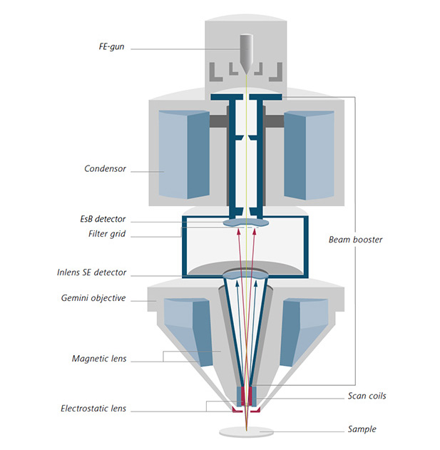
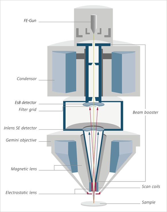
The GeminiSEM family is based on more than 20 years spent perfecting ZEISS Gemini technology. That means you can count on total and efficient detection, excellent resolution and superb ease-of-use. The Gemini objective lens design combines electrostatic and magnetic fields to maximize optical performance while reducing field influences at the sample to a minimum. This enables excellent imaging, even on challenging samples such as magnetic materials. In-lens — the Gemini detection concept — ensures efficient signal detection by detecting secondary (SE) and backscattered (BSE) electrons in parallel. Inlens detectors are arranged on the optical axis, which reduces the need for realignment and thus minimizes time-to-image. Gemini beam booster technology guarantees small probe sizes and high signal-to-noise ratios, right down to very low accelerating voltages. It also minimizes system sensitivity to external stray fields by keeping the beam at high voltage throughout the column until its final deceleration. These advance features — the GEMIN objective, In-lens detection and beam booster technology — are shared by GeminiSEM 360, GeminiSEM 460 and GeminiSEM 560.
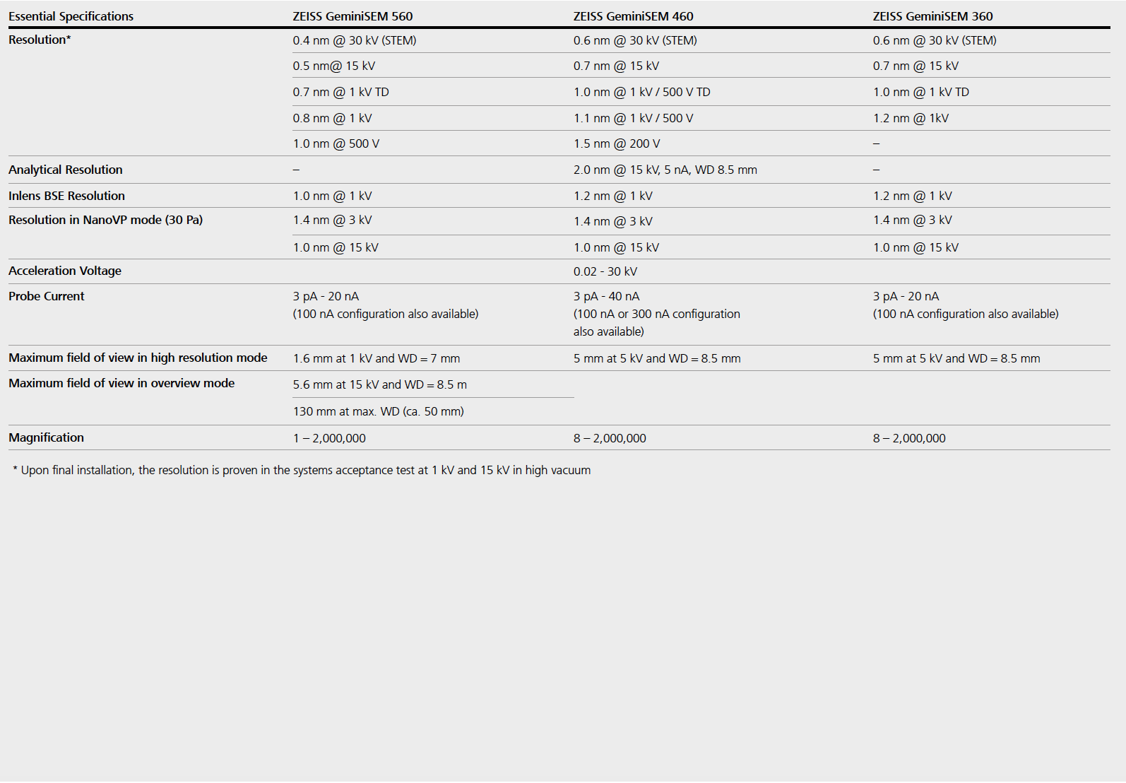
Technical Specifications
Your Benefits Are:
- Long-term stability of the SEM alignment and the effortless way it adjusts all system parameters such as probe current and acceleration voltage.
- Achieve distortion-free, high resolution imaging with the help of the near magnetic-field free optics.
- Get information solely from the top-most layer of your samples with the In-lens SE detector that produces images out of the truly surface sensitive SE 1 electrons true.
- Obtain true material contrast at very low voltages with the detection concept of the Inlens EsB detector.


