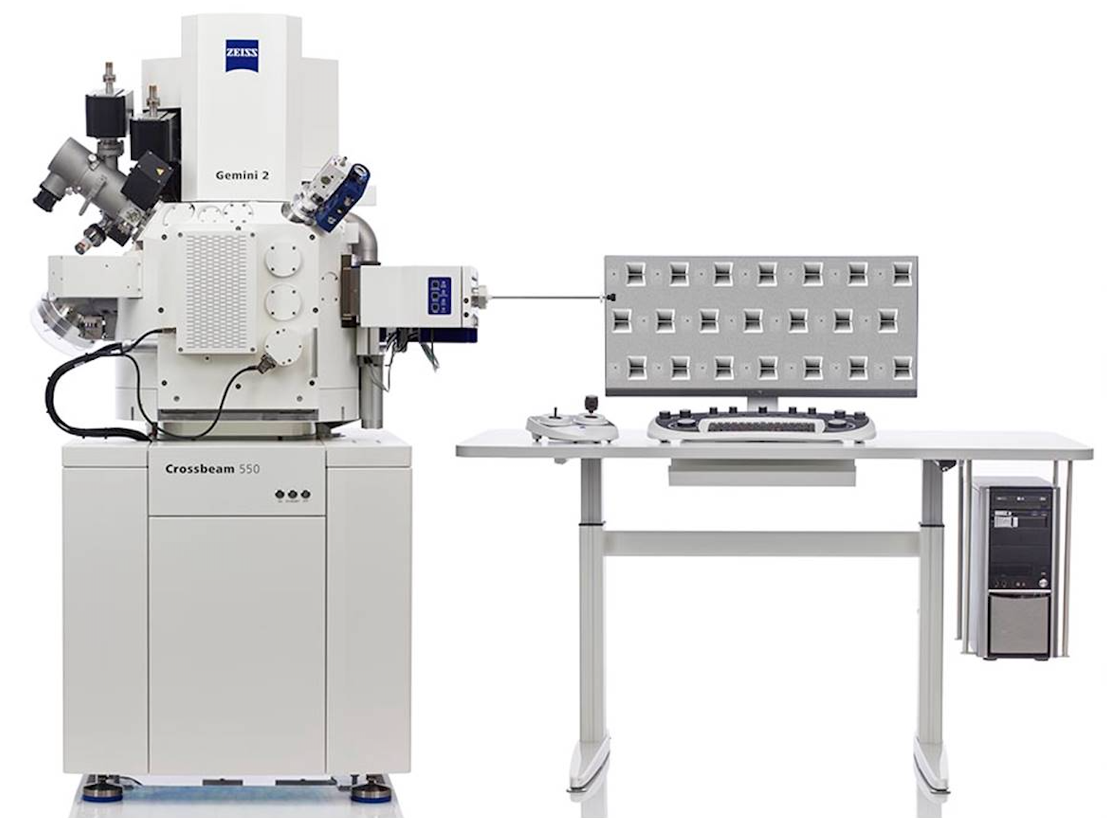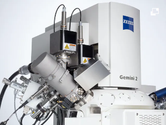
The ZEISS Crossbeam 550L is a large chamber FIB-SEM workstation that provides state of the art e-beam imaging and FIB performance. The system chamber and stage is designed to accommodate a 200mm size sample/wafer and is provided with a fully integrated ZEISS airlock which is designed to accept a 200mm wafer. The Crossbeam delivers sub-nm SEM imaging, ultra thin TEM samples for STEM and TEM characterization, and best in class 3D reconstruction results. Whether your requirements are in Semi-Conductor for Failure Analysis, Industry, Academic and Government Research, the Crossbeams versatility will address all of your requirements, and more.
Unique Features
- Fast and Intuitive TEM Sample Preparation Workflow
- Fast Removal of Material with the ZEISS Ion Sculptor FIB-Column
- Navigation and Accommodation of an 8 inch Wafer
- State of the Art High Resolution End Point Detection with ZEISS Live Imaging
- Best in Class 3D Reconstruction and Analytics
- Best In Class Analytical Flexibility: 3D EDS, 3D WDS, SIMS
- Ease of Use by Design with the ZEISS GEMINI Electron Column
Highlights

Maximize Your SEM Insights
Take advantage of achieving up to 30% better SEM resolution at low voltage.
SEM Performance
- Count on the SEM performance of your ZEISS Crossbeam for 2D surface sensitive images or when performing 3D tomography
- Benefit from high resolution, contrast and signal-to-noise ratios, even when using very low accelerating voltages
- Characterize your sample comprehensively with a range of detectors. Get pure materials contrast with the unique Inlens EsB detector
- Investigate non-conductive specimens undisturbed by charging artifacts.

Increase Your FIB Sample Throughput
Profit from up to 40% faster material removal by the introduction of intelligent FIB milling strategies.
Ion-sculptor FIB
- Use the gallium FIB column Ion-sculptor for a new way of FIB-processing
- Get high quality samples, minimize FIB-induced damage and perform experiments faster at the same time
- Manipulate your samples precisely and fast by using up to 100 nA current without compromising FIB resolution
- Profit from speed and precision of intelligent FIB scanning strategies for material removal and perform your experiments up to 40% faster than before

Experience Best 3D Resolution in Your FIB-SEM Analysis
Enjoy the benefits of integrated 3D analysis for EDS and EBSD investigations.
Expand your Crossbeam
- Expand the capacity of your Crossbeam with ZEISS Atlas 5, the market-leading package for fast, precise tomography
- Perform EDS and EBSD analysis during tomography runs with the integrated 3D Analytics module of ZEISS Atlas 5
- Profit from best 3D resolution and leading isotropic voxel size in FIB-SEM tomography. Probe less than 3 nm in depth and produce surface sensitive, material contrast images using the Inlens EsB detector
- Save time by collecting your serial section images while milling. Take advantage of trackable voxel sizes and automated routines for active control of image quality

