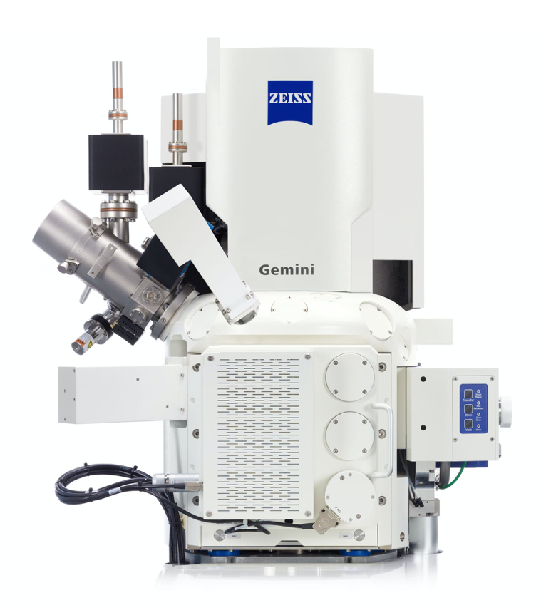
The ZEISS Crossbeam 350 and 550 are the ZEISS medium chamber FIB-SEM workstations. The 350 and 550 provide state of the art e-beam imaging and FIB performance. The system chamber and stage is designed to accommodate a 150mm size sample/wafer and is provided with a fully integrated ZEISS airlock which is designed to accept up to a 200 mm wafer. The Crossbeam delivers sub-nm SEM imaging, ultra thin TEM samples for STEM and TEM characterization, and best in class 3D reconstruction results. Whether your requirements are in Semi-Conductor for Failure Analysis, Industry, Academic and Government Research, the Crossbeams versatility will address all of your requirements, and more.
Unique Features
- Full Integration of the ZEISS Fs Laser Ablation System for Large Material Removal and Machining
- Fast and Intuitive TEM Sample Preparation Workflow
- Fast Removal of Material with the ZEISS Ion Sculptor FIB-Column
- Navigation and Accommodation of samples up to 200mm
- State of the Art High Resolution End Point Detection with ZEISS Live Imaging
- Best in Class 3D Reconstruction and Analytics
- Ease of Use by Design with the ZEISS GEMINI Electron Column

ZEISS Crossbeam Family
Within ZEISS Crossbeam Family you have the choice between Crossbeam 350 or Crossbeam 550. Exploit the variable pressure capabilities of Crossbeam 350 (optional). Or use Crossbeam 550 for your most demanding characterizations and choose the chamber size, standard or large, that best suits your samples.
|
|
ZEISS Crossbeam 350 |
ZEISS Crossbeam 550 |
|
SEM |
Gemini I optics |
|
|
Chamber Size and Ports |
Standard with 18 configurable ports |
Standard with 18 configurable ports |
|
Stage |
100 mm travel range in x/y |
Standard with 100 mm or large |
|
Charge Control |
Flood Gun |
Flood Gun |
|
Exemplified Options |
Inlens SE and Inlens EsB* for simultaneous imaging SE/EsB* imaging |
Inlens SE and Inlens EsB* for simultaneous imaging SE/EsB* imaging |
|
Advantages |
|
High throughput in analytics and imaging, high resolution under all conditions, simultaneous Inlens SE and Inlens EsB* imaging |
|
|
|
* SE secondary electron, EsB energy selective backscatter |
Highlights

Maximize Your SEM Insights
Take advantage of achieving up to 30% better SEM resolution at low voltage.
SEM Performance
- Count on the SEM performance of your ZEISS Crossbeam for 2D surface sensitive images or when performing 3D tomography
- Benefit from high resolution, contrast and signal-to-noise ratios, even when using very low accelerating voltages
- Characterize your sample comprehensively with a range of detectors. Get pure materials contrast with the unique Inlens EsB detector
- Investigate non-conductive specimens undisturbed by charging artifacts.

Increase Your FIB Sample Throughput
Profit from up to 40% faster material removal by the introduction of intelligent FIB milling strategies.
Ion-sculptor FIB
- Use the gallium FIB column Ion-sculptor for a new way of FIB-processing
- Get high quality samples, minimize FIB-induced damage and perform experiments faster at the same time
- Manipulate your samples precisely and fast by using up to 100 nA current without compromising FIB resolution
- Profit from speed and precision of intelligent FIB scanning strategies for material removal and perform your experiments up to 40% faster than before

Experience Best 3D Resolution in Your FIB-SEM Analysis
Enjoy the benefits of integrated 3D analysis for EDS and EBSD investigations.
Expand your Crossbeam
- Expand the capacity of your Crossbeam with ZEISS Atlas 5, the market-leading package for fast, precise tomography
- Perform EDS and EBSD analysis during tomography runs with the integrated 3D Analytics module of ZEISS Atlas 5
- Profit from best 3D resolution and leading isotropic voxel size in FIB-SEM tomography. Probe less than 3 nm in depth and produce surface sensitive, material contrast images using the Inlens EsB detector
- Save time by collecting your serial section images while milling. Take advantage of trackable voxel sizes and automated routines for active control of image quality

