 Rave Scientific
Nanotechnology Instrument Providers and Consultants
- You are here:
- Rave Scientific

- Calibration Standards

- Silicon Finder Grid
Silicon Finder Grid

Overview
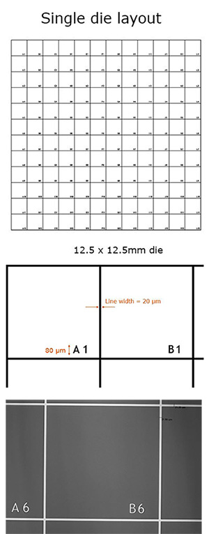
Rave Scientific offers the EM-Tec FG1 silicon SEM finder grid substrate. This substrate consists of an a 12x12mm chrome deposited grid with a 1mm pitch on a conductive ultra-flat silicon substrate. The substrate is divided into 144 indexed fields of 1x1mm where each of the fields has a unique alphanumeric label in the lower right corner. The alphanumeric label is easy to see with a magnifier, stereo microscope and/or SEM. The grid produced is comparable with 25 mesh and is practical for larger particles or small samples mounted on the substrate in separate fields. The EM-Tec FG1 silicon SEM finder grid substrate is ideal for correlative microscopy since the position of the sample is easily located. Size of the EM-Tec FG1 is 12x12mm on a 12.5 x 12.5mm substrate. Primarily designed for SEM applications, but equally suitable for reflected light microscopy, AFM and Auger/SIMS. This unique product has a number of advantages over engraved SEM stubs and the usual copper SEM finder grids:
- Ultra-flat – no height differences such as with copper finder grids
- Pattern is easily visible with unaided eye, SEM and light microscope
- Each individual field is indexed with an alphanumeric label
- Low background signal for SEM imaging – similar to Si chips
- Fine bright pattern over entire area – finer than engraved stubs
- Sample size can be easily judged with the 1x1mm pattern in the background
- Compatible with Ø12.7mm pin stubs, Ø12.2mm JEOL stubs and Ø15mm Hitachi stubs
Easy to mount on SEM and AFM stubs - Compatible with SEM, FIB, AFM, LM, XPS/ESCA, SIMS and Auger
Reusable – solvent resistant and plasma cleaning compatible - The EM-Tec FG1 silicon SEM finder grid substrate in packaged in a clean-room and shipped in a gel-box.
The EM-Tec FG1 finder grid is ideal for:
- Correlative, corroborative, collaborative and repetitive microscopy
- Multi-sample mounting for small samples
- Demonstration samples with quick finder grid
- Quick size estimation with the 1mm grid
Specifications of the pattern and the ultra-flat silicon wafer of the EM-Tec FG1 silicon finder grid:
| Pattern size | 12 x12 mm divided into 144 individual 1x1mm fields |
| Numbering | Each field has unique alphanumeric label in lowe right corner |
| Pattern/labels | 75nm thick deposited Cr with 20µm line width, 80µm label height |
| Substrate size | 12.5x12.5mm |
| Orientation | |
| Type | P (Boron) |
| Resistance | 1-10 Ohm/cm |
| Grade | Prime / CZ Virgin |
| Coating | None, native oxide only |
| Thickness | 675µm (+/- 20µm) |
| TTV | ≤1.5µm |
| Warp | ≤30µm |
- SEM Sample Holders
- (Overview of Sample Holders)
- Angled and Tilt holders
- Bulk SEM sample holders
- Centering vise holder
- C-Square Muti Pin Holders
- Compact and universal vises
- EBSD sample holders
- FIB grid holders
- Filter Disk Holders
- Geological slide holders
- Gripping stub & stub vises
- Metallographic standard and reference sample holders
- Multiple Hitachi stub holders
- Multiple JEOL stub holders
- Multiple pin stub holders
- Multi XL holder large
- Non Magnetic Sample Holders
- S Clip Sample Holders
- Sample Clamp holders
- Small sample holders
- Small vise holders
- Soft jaw lining kit
- STEM imaging holder
- Swivel tilt sample holders
- TEM grid holders
- Transmission EBSD sample holders for TEM and FIB grids
- Universal sample holder kit
- Versa-Plate Adaptable Holder
- Versatile vise clamp holders
- Wafer holders
- XT stage extender strips
- °360°/90°off-set holder
- Metallographic Mount Holders
- Multiple Metallographic Mount Holders
- Sample Preparation
- Overview-Sample Preparation
- Applicators and Swabs
- Carbon Rods & Fibers
- Conductive Adhesives
- Cutting Tools
- Gloves & Cleaning Supplies
- Lab Scissors
- Non-Conductive Adhesives
- Plastic Transfer Pipettes
- Preparation Mats and Tiles
- Probes and Picks
- SEM Preparation Stands
- SEM-TEM Remote Plasma Cleaner - IBSS Plasma
- Sputter Targets
- Stainless Steel Mesh
- Supports and Substrates
- Tweezers
- Overview Tweezers
- High Precision Tweezers
- High Prec. Reverse Tweezers
- High Prec. Locking Tweezers
- High Prec. Mini Tweezers
- High Prec. Slim tweezers
- High Prec. Titanium Tweezers
- High Pr. Super Alloy Tweezers
- Cutting Tweezers
- SEM Stub Gripper Tweezers
- Cryo Grid Box Tweezers
- AFM/SPM cantilever tweezers
- AFM/SPM Disc tweezers
- Gatan 3View Pin Tweezers
- Wafer Handling Tweezers
- Plastic Tweezers
- Repl. Plastic Tip Tweezers
- Repl. ESD Ceramic Tip Tw.
- Repl. Ceramic Tips Tw.
- Value-Tec Fine Tweezers
- Value-Tec Ceramic Tip Tw.
- Value-Tec Fibre Grip Tweezers
- Value-Tec Strong Tweezers
- Tools
- Conductive SEM Coating Fluid
- PHP-4 Array Tomography Automated Kapton Tape Glow Discharge Cleaner
- MC-4 Multi-Modular Cleaner: UV Light, Plasma and Heating for SEM and TEM Samples
- EM Filaments
- SEM Sample Stubs
- Sample Stub Adapters
- JEOL SEM Supplies
- Overview JEOL SEM Supplies
- JEOL Tungsten Filaments
- Vacuum Storage-JEOL
- JEOL SEM Sample Holders
- JEOL Calibration Standards
- Desktop-NEOSCOPE SEM Supplies
- Desktop-NEOSCOPE SEM Holders
- JEOL Multi-Stub Holders
- JEOL Denka Lab6 Emitters
- JEOL Particle Analysis Holders
- JEOL SEM Stubs
- JEOL SEM Holder Adapters
- Sample Preparation Stands-JEOL
- Sample Storage-JEOL
- In-Situ Chamber Plasma Cleaner-JEOL
- SEM Stub Gripper-JEOL
- Hitachi SEM Supplies
- Overview Hitachi SEM Supplies
- Hitachi Calibration Standards
- HITACHI TM Desktop SEM Supplies
- HITACHI TM Desktop SEM Holders
- HITACHI -In Lens Sample Stubs
- HITACHI Multiple Stub SEM Holders
- HITACHI Particle Analysis Holders
- HITACHI M4 Stubs
- HITACHI SEM Holder Adapters
- HITACHI Tungsten Filaments
- Sample Preparation Stands-HITACHI
- Sample Storage-HITACHI
- HITACHI Sample Holders
- Vacuum Storage-HITACHI
- In-Situ Chamber Plasma Cleaner-Hitachi
- SEM Stub Gripper-Hitachi
- Zeiss SEM Supplies
- Overview
- Calibration Standards Zeiss
- Zeiss SEM Holders
- Zeiss Sample Preparation Stands
- Zeiss Tungsten Filaments
- Zeiss Denka Lab6 Filaments
- Zeiss Denka 174 Schottky Emitters
- Vacuum Storage-Zeiss
- Zeiss Pin Stubs
- Sample Storage-Zeiss
- Zeiss SEM Holder Adapters
- Zeiss Particle Analysis Holders
- In-Situ Chamber Plasma Cleaner
- SEM Stub Gripper Tweezers-Zeiss
- Thermo-FEI SEM Supplies
- Overview Thermo-FEI Supplies
- Calibration Standards-Thermo-FEI
- Dual Beam TEM Grids
- Gallium LMIS-Thermo FEI
- Dual Beam Pre-Cursors
- Dual Beam TEM Grid Holders
- Dual Beam Low Profile Stubs
- FEI Dual beam EBSD-3D sample Holder
- Dual Beam Gallium Sources
- FESEM FEI XL & Sirion Source Changes
- Non Magnetic Sample Holders
- Phenom SEM Supplies-Thermo-FEI
- Phenom Tabletop SEM Stubs & Sample Holders
- SEM Sample Holders-Thermo-FEI
- SEM Pin Stubs-Thermo-FEI
- Stage Adapters-Thermo FEI
- Thermo-FEI Tungsten Filaments
- SEM Stub Grippers-Thermo-FEI
- Particle Analysis Holders-Thermo FEI
- TESCAN SEM Supplies
- Overview TESCAN SEM Supplies
- Sample Preparation Stands-TESCAN
- Calibration Standards-TESCAN
- TESCAN SEM Sample Holders
- TESCAN Tungsten Filaments
- TESCAN Denka Lab6 Cathode
- TESCAN Denka 174 TFE Emitters
- TESCAN Particle Analysis Holders
- TESCAN SEM Holder Adapters
- TESCAN SEM Stubs
- Sample Storage-TESCAN
- Vacuum Storage-TESCAN
- TESCAN FIB-SEM TEM Lift-Out Grids
- TESCAN FIB-SEM TEM Grid Holders
- TESCAN FIB-SEM Pre-Tilt Low Profile Stubs
- SEM Stub Gripper Tweezers-TESCAN
- Desktop SEM Supplies
- Vacuum Supplies
- Light Microscopy Supplies
- Sputter Targets
- Sample Storage
- Overview
- Vacuum Sample Storage
- Inert Gas Sample Storage
- Rave-Tec Membrane Boxes
- Rave-Tec Sticky Gel Carrier Boxes
- Vacuum Glass Storage
- Pin Stub Storage
- Hitachi M4 Storage Boxes
- JEOL Stub Storage Boxes
- Desiccant Box
- Barrier Foil Ziplock Bags
- Wafer Carrier Trays
- Clear Plastic Boxes
- Small Cardboard Boxes
- Magn. AFM Disc Boxes
- Rave-Tec Field and lab sampler kits and boxes
- SEM Vacuum Transfer Shuttle for air-sensitive samples
- Vacuum Transfer Test
- SEM Stage Adapters
- Cryo Supplies
- Calibration Standards
- Dual Beam Supplies
- TEM Supplies
- AFM Supplies
- Lab Supplies
- SEM Sputter Coaters
- Safematic Supplies
- Metallurgical Supplies Overview
- Compact Smart Clip Metallographic Mount Holders for SEM
- Sample Embedding Clips
- Silicone Embedding Cups
- MET-C conductive hot embedding resin powder
- Laboratory Handheld Engraving Tool & Engraving Pen
- Rave-Tec temporary mounting waxes
- Vacuum Desiccators
- Diamond Polishing Paste-Metallurgical
- PTFE beakers-Metallurgical
- Metallurgical EBSD Holders
- SEM Stage Adapters Overview
- Vacuum Products
- Edwards Vacuum Supplies
- Pfeiffer Vacuum Products
- Pfeiffer Helium Leak Detectors
- Edwards Helium Leak Detectors
- Rotary Pump Vacuum Oil
- Apiezon Vacuum Grease
- Krytox Vacuum Grease
- KF / NW Vacuum Flange Connection Hardware
- Hysol 1C / Torr Seal Vacuum Epoxy Resin Sealant kit
- Rave-Tec stainless steel vacuum chamber for degassing
- Silver and carbon conductive vacuum greases
- Metal wires and materials for vacuum evaporation
- Rave-Tec KF/NW stainless steel vacuum bellows
