 Rave Scientific
Nanotechnology Instrument Providers and Consultants
- You are here:
- Rave Scientific

- Rave Shop

- Sample Preparation Supplies

- Supports and Substrates

- Silicon Wafers and Chips
Overview
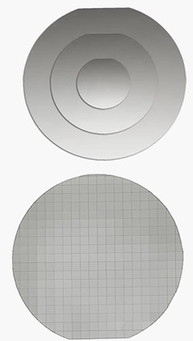
Polished silicon is an excellent substrate for imaging, experiments, nanotechnology and micro-fabrication applications. It is available in the form of wafers, diced wafer or as smaller chips (pieces). The silicon wafer and chips all have a orientation. Cleaving of the wafers to the desired size with a orientation wafers is straight forward and simple. The silicon wafers and chips are all P-type, doped with B to provide excellent conductivity for SEM, FIB and STM applications.
For biological applications silicon resembles glass, which makes it a suitable support for growing and/or mounting cells. For imaging applications, it is an ideal sample substrate for small particles due to the low background signal of the highly polished surface.
Two grades of silicon substrates are offered:
Micro-Tec standard silicon wafers and silicon chips for standard application and medium resolution imaging.
Nano-Tec ultra-flat silicon wafers and ultra-flat silicon chips for demanding applications and high resolution imaging.
Micro-Tec <P/100> standard silicon wafers and diced wafer for SEM substrates
The Micro-Tec <P/100> silicon wafer substrates can be used for sample substrates, micro-fabrication, substrate for thin film research or biological substrates. Useful flat substrate for SEM imaging of particles due to the low background. For biological applications, Si has similar properties as glass and can be used to mount or grow cells. Can be easily cleaved or used as a whole wafer. The Micro-Tec Si wafers are packed in a wafer carrier tray sfor protection. The diced wafer supplied on wafer adhesive disc and packed between two plastic sheets for protection. The Si chips can be easily lift off the adhesive sheet.
The Micro-Tec standard silicon wafer substrates are available as:
- SEM Sample Holders
- (Overview of Sample Holders)
- Angled and Tilt holders
- Bulk SEM sample holders
- Centering vise holder
- C-Square Muti Pin Holders
- Compact and universal vises
- EBSD sample holders
- FIB grid holders
- Filter Disk Holders
- Geological slide holders
- Gripping stub & stub vises
- Metallographic standard and reference sample holders
- Multiple Hitachi stub holders
- Multiple JEOL stub holders
- Multiple pin stub holders
- Multi XL holder large
- Non Magnetic Sample Holders
- S Clip Sample Holders
- Sample Clamp holders
- Small sample holders
- Small vise holders
- Soft jaw lining kit
- STEM imaging holder
- Swivel tilt sample holders
- TEM grid holders
- Transmission EBSD sample holders for TEM and FIB grids
- Universal sample holder kit
- Versa-Plate Adaptable Holder
- Versatile vise clamp holders
- Wafer holders
- XT stage extender strips
- °360°/90°off-set holder
- Metallographic Mount Holders
- Multiple Metallographic Mount Holders
- Sample Preparation
- Overview-Sample Preparation
- Applicators and Swabs
- Carbon Rods & Fibers
- Conductive Adhesives
- Cutting Tools
- Gloves & Cleaning Supplies
- Lab Scissors
- Non-Conductive Adhesives
- Plastic Transfer Pipettes
- Preparation Mats and Tiles
- Probes and Picks
- SEM Preparation Stands
- SEM-TEM Remote Plasma Cleaner - IBSS Plasma
- Sputter Targets
- Stainless Steel Mesh
- Supports and Substrates
- Tweezers
- Overview Tweezers
- High Precision Tweezers
- High Prec. Reverse Tweezers
- High Prec. Locking Tweezers
- High Prec. Mini Tweezers
- High Prec. Slim tweezers
- High Prec. Titanium Tweezers
- High Pr. Super Alloy Tweezers
- Cutting Tweezers
- SEM Stub Gripper Tweezers
- Cryo Grid Box Tweezers
- AFM/SPM cantilever tweezers
- AFM/SPM Disc tweezers
- Gatan 3View Pin Tweezers
- Wafer Handling Tweezers
- Plastic Tweezers
- Repl. Plastic Tip Tweezers
- Repl. ESD Ceramic Tip Tw.
- Repl. Ceramic Tips Tw.
- Value-Tec Fine Tweezers
- Value-Tec Ceramic Tip Tw.
- Value-Tec Fibre Grip Tweezers
- Value-Tec Strong Tweezers
- Tools
- Conductive SEM Coating Fluid
- PHP-4 Array Tomography Automated Kapton Tape Glow Discharge Cleaner
- MC-4 Multi-Modular Cleaner: UV Light, Plasma and Heating for SEM and TEM Samples
- EM Filaments
- SEM Sample Stubs
- Sample Stub Adapters
- JEOL SEM Supplies
- Overview JEOL SEM Supplies
- JEOL Tungsten Filaments
- Vacuum Storage-JEOL
- JEOL SEM Sample Holders
- JEOL Calibration Standards
- Desktop-NEOSCOPE SEM Supplies
- Desktop-NEOSCOPE SEM Holders
- JEOL Multi-Stub Holders
- JEOL Denka Lab6 Emitters
- JEOL Particle Analysis Holders
- JEOL SEM Stubs
- JEOL SEM Holder Adapters
- Sample Preparation Stands-JEOL
- Sample Storage-JEOL
- In-Situ Chamber Plasma Cleaner-JEOL
- SEM Stub Gripper-JEOL
- Hitachi SEM Supplies
- Overview Hitachi SEM Supplies
- Hitachi Calibration Standards
- HITACHI TM Desktop SEM Supplies
- HITACHI TM Desktop SEM Holders
- HITACHI -In Lens Sample Stubs
- HITACHI Multiple Stub SEM Holders
- HITACHI Particle Analysis Holders
- HITACHI M4 Stubs
- HITACHI SEM Holder Adapters
- HITACHI Tungsten Filaments
- Sample Preparation Stands-HITACHI
- Sample Storage-HITACHI
- HITACHI Sample Holders
- Vacuum Storage-HITACHI
- In-Situ Chamber Plasma Cleaner-Hitachi
- SEM Stub Gripper-Hitachi
- Zeiss SEM Supplies
- Overview
- Calibration Standards Zeiss
- Zeiss SEM Holders
- Zeiss Sample Preparation Stands
- Zeiss Tungsten Filaments
- Zeiss Denka Lab6 Filaments
- Zeiss Denka 174 Schottky Emitters
- Vacuum Storage-Zeiss
- Zeiss Pin Stubs
- Sample Storage-Zeiss
- Zeiss SEM Holder Adapters
- Zeiss Particle Analysis Holders
- In-Situ Chamber Plasma Cleaner
- SEM Stub Gripper Tweezers-Zeiss
- Thermo-FEI SEM Supplies
- Overview Thermo-FEI Supplies
- Calibration Standards-Thermo-FEI
- Dual Beam TEM Grids
- Gallium LMIS-Thermo FEI
- Dual Beam Pre-Cursors
- Dual Beam TEM Grid Holders
- Dual Beam Low Profile Stubs
- FEI Dual beam EBSD-3D sample Holder
- Dual Beam Gallium Sources
- FESEM FEI XL & Sirion Source Changes
- Non Magnetic Sample Holders
- Phenom SEM Supplies-Thermo-FEI
- Phenom Tabletop SEM Stubs & Sample Holders
- SEM Sample Holders-Thermo-FEI
- SEM Pin Stubs-Thermo-FEI
- Stage Adapters-Thermo FEI
- Thermo-FEI Tungsten Filaments
- SEM Stub Grippers-Thermo-FEI
- Particle Analysis Holders-Thermo FEI
- TESCAN SEM Supplies
- Overview TESCAN SEM Supplies
- Sample Preparation Stands-TESCAN
- Calibration Standards-TESCAN
- TESCAN SEM Sample Holders
- TESCAN Tungsten Filaments
- TESCAN Denka Lab6 Cathode
- TESCAN Denka 174 TFE Emitters
- TESCAN Particle Analysis Holders
- TESCAN SEM Holder Adapters
- TESCAN SEM Stubs
- Sample Storage-TESCAN
- Vacuum Storage-TESCAN
- TESCAN FIB-SEM TEM Lift-Out Grids
- TESCAN FIB-SEM TEM Grid Holders
- TESCAN FIB-SEM Pre-Tilt Low Profile Stubs
- SEM Stub Gripper Tweezers-TESCAN
- Desktop SEM Supplies
- Vacuum Supplies
- Light Microscopy Supplies
- Sputter Targets
- Sample Storage
- Overview
- Vacuum Sample Storage
- Inert Gas Sample Storage
- Rave-Tec Membrane Boxes
- Rave-Tec Sticky Gel Carrier Boxes
- Vacuum Glass Storage
- Pin Stub Storage
- Hitachi M4 Storage Boxes
- JEOL Stub Storage Boxes
- Desiccant Box
- Barrier Foil Ziplock Bags
- Wafer Carrier Trays
- Clear Plastic Boxes
- Small Cardboard Boxes
- Magn. AFM Disc Boxes
- Rave-Tec Field and lab sampler kits and boxes
- SEM Vacuum Transfer Shuttle for air-sensitive samples
- Vacuum Transfer Test
- SEM Stage Adapters
- Cryo Supplies
- Calibration Standards
- Dual Beam Supplies
- TEM Supplies
- AFM Supplies
- Lab Supplies
- SEM Sputter Coaters
- Safematic Supplies
- Metallurgical Supplies Overview
- Compact Smart Clip Metallographic Mount Holders for SEM
- Sample Embedding Clips
- Silicone Embedding Cups
- MET-C conductive hot embedding resin powder
- Laboratory Handheld Engraving Tool & Engraving Pen
- Rave-Tec temporary mounting waxes
- Vacuum Desiccators
- Diamond Polishing Paste-Metallurgical
- PTFE beakers-Metallurgical
- Metallurgical EBSD Holders
- SEM Stage Adapters Overview
- Vacuum Products
- Edwards Vacuum Supplies
- Pfeiffer Vacuum Products
- Pfeiffer Helium Leak Detectors
- Edwards Helium Leak Detectors
- Rotary Pump Vacuum Oil
- Apiezon Vacuum Grease
- Krytox Vacuum Grease
- KF / NW Vacuum Flange Connection Hardware
- Hysol 1C / Torr Seal Vacuum Epoxy Resin Sealant kit
- Rave-Tec stainless steel vacuum chamber for degassing
- Silver and carbon conductive vacuum greases
- Metal wires and materials for vacuum evaporation
- Rave-Tec KF/NW stainless steel vacuum bellows
