Proper Target Material Selection when Coating Samples Using an SEM Sputter Coater
In this article, we will identify target material options for use in your specimen coater when analyzing a non-conductive sample.
In order to optimize performance with electron beam imaging, coating an SEM sample with a conductive metal renders non-conductive SEM samples conductive and avoids charging of the sample surface. This in turn enables higher sample stability under the electron beam and higher resolution imaging. In most cases, coating SEM samples with only a nanometer of a conductive material increases the signal to noise ratio dramatically, thus resulting in crisp and clear images. Proper target material selection is dictated by overall imaging requirements and the materials being studied. This article will act as a guide to determine the ideal target materials to use for general electron beam imaging as well as EDX analysis.
Introduction
Since its commercial introduction in 1965, the electron microscope has evolved over the past 50 years with vast improvements and yet some of the sensitivity of imaging and analyzing non-conductive materials remains. The end user is still required today to manage this sensitivity when working with non-conductive materials. Fortunately, today, the EM user has a number of options to aid in this process.
The most dependable approach, guaranteeing the best performance under electron beam imaging, is to coat the non-conductive sample with a target material. A coating material for making a non-conductive SEM sample conductive should be selected to achieve optimum performance. Sputter coating materials can vary for different sample materials and their desired results. Most SEM sputter coaters allow for an easy and quick target change, thus allowing for the selection of various options with minimal effort.
The sputter coating quality is affected by the target material, process parameters and by the interaction with the sample material. Coating an SEM sample with a highly conductive metal makes non-conductive SEM samples conductive to avoid charging of the sample surface. This results in higher resolution imaging due to higher sample stability under the electron beam. In most cases, coating SEM samples with only a nanometer of a conductive material increases the signal to noise ratio dramatically, resulting in crisp and clear images. Considering that most coating materials have a much higher secondary electron (SE) yield than the non-conductive sample materials, the results are greatly improved.
Materials and Methods
The following is a list of materials that can be used to sputter coat samples for the SEM. This should not be considered as an exhaustive list. Keep in mind that this information is only valid when using a modern DC magnetron SEM sputter coater with Argon as process gas.
Gold
Gold is the most widely used coating material to coat non-conductive samples for standard SEM applications. Due to its low work function it is a very efficient to coat. When using cool sputter coaters while sputtering thin layers, there is hardly any heating of the sample surface. The grain size is visible (relatively large grain size) when using high magnifications on modern SEMs. Gold can be used for low and medium magnification applications and is an ideal coating material for low resolution imaging. The L and M of Au lines can interfere with EDX analysis.
Gold/Palladium
The Au/Pd alloy (60/40 and 80/20) is less efficient to coat with than using pure gold, which results in lower sputter rates. There is a slight difference between Au and Au/Pd in that the latter offers a slightly smaller sputtered grain size. This material is less suitable for EDX analysis due to the extra set of peaks for Pd, which can interfere with lighter elements.
Silver
Ag is a most suitable and lower cost alternative for Au in many imaging applications for low and medium magnifications ranges. It is a widely underestimated coating material. Ag has the highest conductivity of all metals. When using EDS, Ag is an alternative for Au on many biological samples if P, Cl and S need to be analyzed, though it can also interfere with lighter element detection. The sputtering rate is similar to Au, the SE yield is somewhat lower than for Pt, Au or Ir. The grain sizes are similar or slightly larger than Au (except for samples containing halogens which can exhibit coarser grains). The Ag coating can tarnish (in the presence of halogens) and is less suitable for long term storage. Ag is an excellent low-cost coating material for low to intermediate resolution imaging.
Platinum
Pt has a finer grain size than Au or Au/Pd and is therefore more suitable for higher magnification applications. Sputtered Pt results in an excellent SE yield. The higher work function results in a lower sputtering rate than for Au. Pt tends to be sensitive for "stress cracking" when oxygen is present. Pt is more expensive than Au due to higher fabrication costs. Keep in mind the characteristic x-rays of Pt and its potential to overlap with the materials of interest in your sample.
Platinum/Palladium
Pt/Pd alloy (80/20) has a similar small grain size and SE yield as pure Pt, but it is less sensitive to "stress cracking". Pt/Pd is a suitable all-round coating material for FESEM applications when thin coatings are used. Keep in mind that there are more characteristic x-rays then Pt alone.
Iridium
Ir exhibits a very fine grain size on virtually all materials and is an excellent all-round fine grain coating material for FESEM applications. It is the material of choice for high and ultra-high resolution FESEM imaging. With the added benefit of being a non-oxidizing material and a high SE yield, it has been replacing Chromium for high resolution sample coating. It requires the use of a high-resolution sputter coater and it has lower sputtering rates. The targets are thicker due to fabricated constraints, but overall costs are lower than for Pt or Pt/Pd. Ir is also an excellent alternative coating material for coating samples which have to be analyzed for carbon by EDX (or WDX). A thin layer is enough to create excellent conductivity and since the material is very rare it hardly interferes with EDX (or WDX) analysis.
Chromium
Cr has a very fine grain size, especially on semiconductor type materials and has proven to be a useful coating material for FESEM applications. Cr requires the use of a turbo pump, high vacuum (high resolution sputter coater with a target shutter for target conditioning to remove the oxide). The higher vacuum, in combination with pure Argon flushing of the chamber, reduces the partial pressure of oxygen, enough to avoid oxidization of the sputtered Cr layer. The Cr on the sample surface will oxidize in air and samples must be viewed immediately after coating. (Samples can be stored in high vacuum.) Cr has lower sputtering rates and the target tends to heat up. Cr is an excellent coating material for high resolution BSE imaging of low Z and biological samples. Cr can be a good choice for EDX analysis, keeping in mind the potential for low z interference and oxygen in the deposited sputtered film.
Tungsten
W is an excellent alternative for high-resolution coating. W has a very fine grain size and tends to be less visible than Cr. W oxidizes rapidly, similar to Cr. Low sputtering rates, but SE yield tends to be higher. Samples must be imaged immediately after coating due to potential oxidization. W has a wide range of potential EDX interference, and the potential for oxygen in the deposit can interfere with low end analysis.
Tantalum
Ta is also candidate for high resolution coating (most refractory and high melting metals exhibit a finer grain size). Ta oxidizes quite rapidly, similar to Cr. Low sputtering rates, but due to its high atomic number, the SE yield tends to be higher. Samples must be imaged immediately after coating or stored under high vacuum. The potential for oxygen can be misleading in EDX.
Palladium
Pd has been used as a lower cost alternative for low to medium magnification ranges. Depending upon the cost of Pd, it can be a lower cost alternative to Au. Pd coatings gives a lower SE signal than Au. When using EDX analysis, Pd can also be an alternative. Like Au, Pd has a large potential for EDX interference due to its wide range of characteristic x-ray line.
Nickel
Ni is an alternative coating material for EDX applications and BE imaging. Not ideal for SE imaging, the coating oxidizes slowly. Considering Ni as a magnetic material, it can "short circuit" the magnet in the DC magnetron sputter resulting in a less dense plasma (lowering the deposition rates). In a standard SEM sputter coater, the coating contains a mixture of Ni and Ni-oxide. Turbo pumped systems can reduce the presence of Ni-oxide. The presence of the oxide in the deposit, could have a deleterious effect on low z EDX analysis.
Copper
Cu is an alternative low-cost material for EDX applications and BE imaging. Suitable for low and medium magnification ranges, but the SE yield is lower. The Cu sputtered coatings will slowly oxidize. In a standard SEM coater, the coating consists of a mixture of Cu and Cu-oxide and higher vacuum deposition system can reduce the presence of Cu-oxide. The presence of the oxide in the deposit could have a deleterious effect on low z EDX analysis.
Titanium
Ti is rarely used as coating material, but it has applications where it is chosen to avoid any interference with EDX analysis (consider the presence of its oxide). Low atomic number gives less interference with BSE imaging. Ti oxidizes quite rapidly and samples need to be imaged immediately after coating.
Results
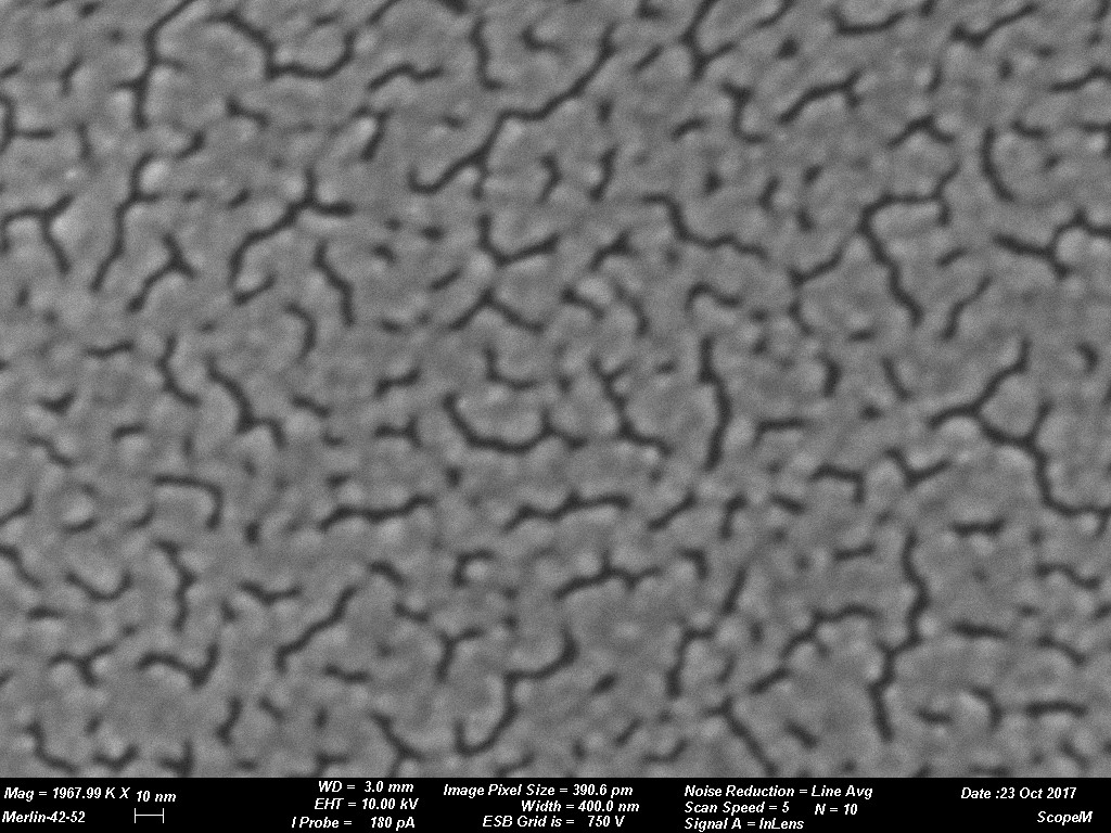
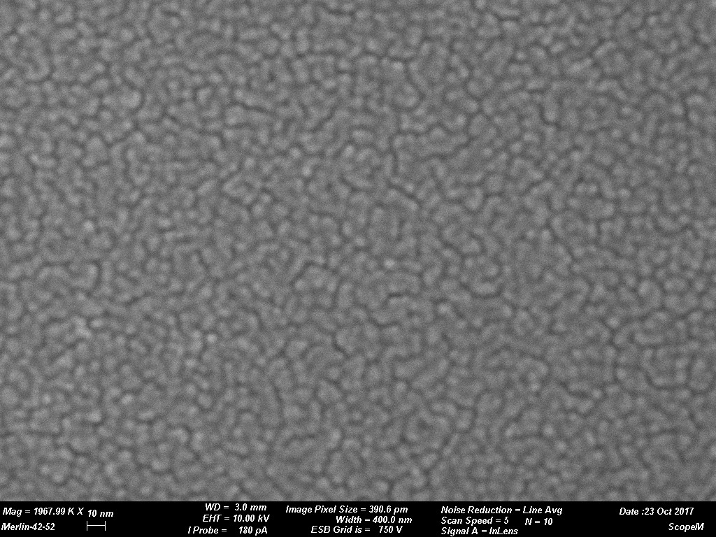
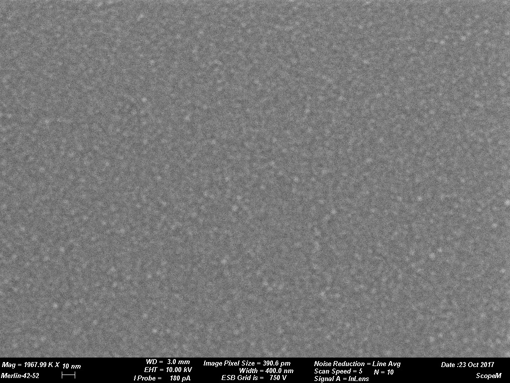
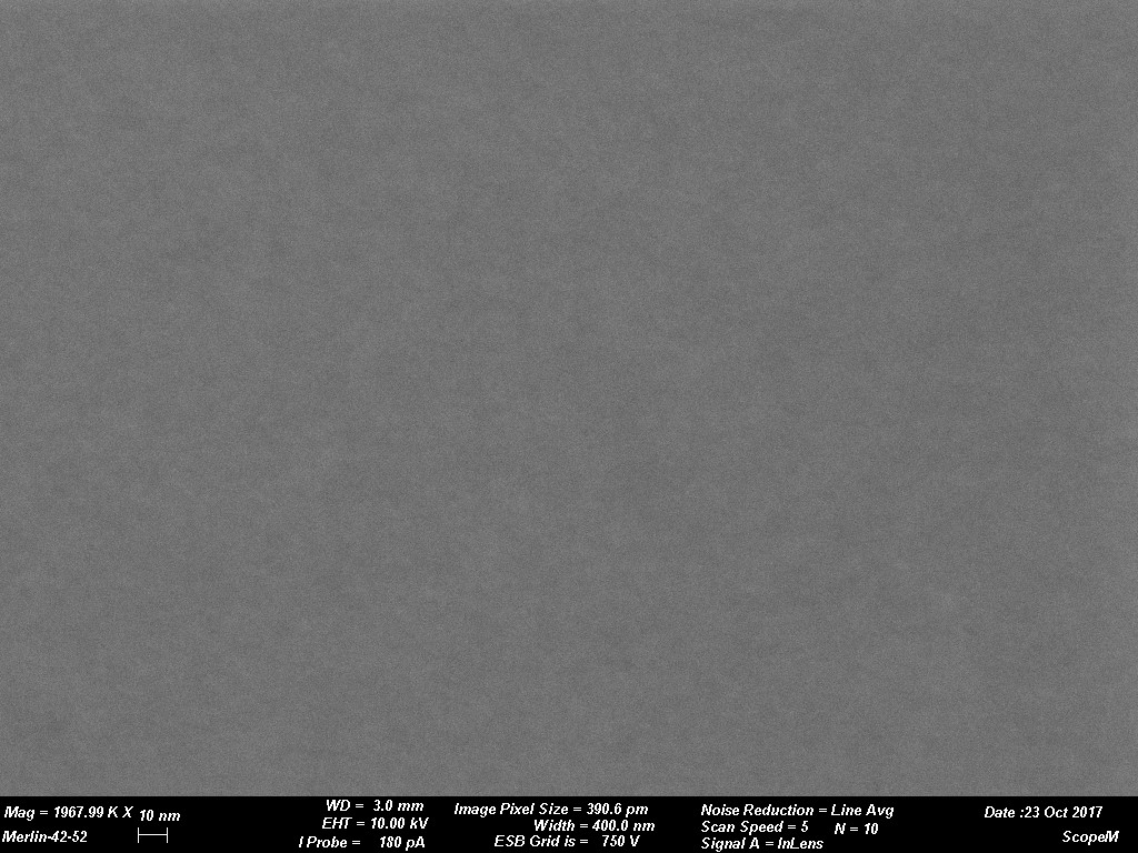
Figures 1 through 4 are examples of grain size variations dependent on various sputtering targets. The sputtered films were produced using a CCU-010 HV (turbo pumped) Safematic Coating System on glass slides. Film thickness measurements were obtained using the quartz thickness monitor (operating at 6 M Hz) inherent with the system. Images were obtained on a Zeiss Merlin SEM at the same magnifications for all images. (Relevant operating parameters can be found in the data bar on each image.) Figure 1 reveals the surface structure of a sputtered Au film while Figures 2 through 4 reveal Au-Pd, Cr and W respectively. Variations of grain size is evident. The grain size of the deposit is seen to decrease in each subsequent image.
Discussion
The tables below provide practical guidance information for selecting the target material and expected grain size of the coating. The information is only valid when using a modern DC magnetron SEM sputter coater with Argon as process gas. Grain size of the coating depends strongly on coating thickness and coating material/sample material interaction. As a rule, the thinner the coating the smaller the grain size will be. It must be considered that if the surface has significant and irregular topography a uniform coating might not be a reality. This could result in localized surface charging which could degrade imaging efficiency. This could be rectified if a tilting rotating/planetary type of stage was available in the sputter coating system. Using standard coating conditions and coating similar sample materials the following grain sizes can be expected. When considering rendering a sample conductive for study by SEM grain size of the sputtered deposit is a key issue. The grain size can have an impact on imaging resolution. Table 1 reveals a few typical grain sizes of sputtered deposits under similar conditions. Figure 1 through Figure 4 are examples of grain size variations dependent on various sputtering targets.
If EDX analysis of the sample is needed, try to select a coating (target) material which is not present in the sample. This would avoid overlapping peaks in the EDX spectrum and confusion within the EDX analysis. Also consider all the lines in your sample (K, L, M) and those of the sputtered film in conjunction with the accelerating voltage of the electron beam. It must be kept in mind what lines could be present, but also what line will be present (and potentially enhanced) with your beam operating voltage used in the study.
A sputter deposition selection guide for target materials for SEM/FESEM imaging and EDX applications is summarized in Table 2. In general, few metals are suitable for EDX analysis due to their wide range of interference. Knowing the general composition of your unknown is a good guideline but, not practical. If this information is known, then metal target selection can accommodate the analysis. If not, then Carbon deposition (evaporation) is the recommended approach to render a nonconductive sample amenable for EDX analysis.
Conclusion
Today’s sputter coating systems allows the user to customize his/her sample preparation for their investigation(s). The general ease with which the target(s) can be varied allows for a large degree of flexibility for accommodating the sample being analyzed. This can address interest in low or high imaging resolution, cost of target material(s) and EDX analysis to a certain degree. Different sputter targets can require additional infrastructure such as increased pumping/vacuum capabilities or preconditioning of the target with a shudder system. The information presented here is just a general guideline for planning your next steps for sample preparation when considering imaging in conjunction with EDX analysis.
| Table 1 | Coating Thickness |
|---|---|
| Gold, silver | 5-10nm |
| Palladium | 5-10nm |
| Gold/Palladium | 4-8nm |
| Platinum | 2-3nm |
| Iridium | 1-2nm |
| Chromium | 1-2nm |
| Tungsten | <1nm |
| Table 2 | ||||||||||||||
|---|---|---|---|---|---|---|---|---|---|---|---|---|---|---|
| Target Materials | ||||||||||||||
| Application | Au | Au/Pd | Ag | Pt | Pt/Pd | Ir | Cr | W | Ta | Pd | Ni | Cu | Ti | C* |
| Low and medium magnifications | x | x | x | x | x | x | - | - | - | x | x | x | - | x |
| High resolution imaging | - | - | - | x | x | x | x | x | x | - | - | - | - | x |
| Ultra-high resolution imaging | - | - | - | - | x | x | x | x | x | - | - | - | - | x |
| SE signal boost (1nm or less) | x | - | - | x | - | x | - | - | - | - | - | - | - | - |
| BSE imaging | - | - | - | - | - | - | x | - | - | x | - | - | - | x |
| Table top SEM coating with air | x | - | - | - | - | - | - | - | - | - | - | - | - | - |
| Gold colloids imaging | - | - | - | - | - | - | x | - | - | - | - | - | - | x |
| EDX analysis | - | - | - | - | - | - | x | - | - | - | x | x | x | x |
| Light element analysis | - | - | - | - | - | x | - | - | - | - | - | - | - | - |
| EBSD (2-3nm) | x | - | - | x | - | x | - | x | - | - | - | - | - | x |
| * C (Carbon) deposited by evaporation, not discussed here | ||||||||||||||
References
General Book References:
J Goldstein, et. al., Scanning Electron Microscopy and X-ray Microanalysis, Kluwer Academic/Plenum Press, New York, 2003.
D Newbury, et. al., Advanced Scanning Electron Microscopy and X-Ray Microanalysis, Plenum Press, New York, 1986.
BL Gabriel, SEM: A User’s Manual for Materials Science, America Society for Metals, Metals Park, Ohio, 1985.
Conversations with Jack Vermuelin of Micro to Nano, Haarlem, North Holland Province, Netherlands.
Images courtesy of Dr. Joakim Reuteler, ScopeM, ETH Zurich.