Scanning Electron Microscope
Overview
The scanning electron microscope (SEM) uses a focused beam of high-energy electrons to generate a variety of signals at the surface of the specimen. There are a number of by-products of signal that result in the electron-sample interaction that reveal information about the sample. This includes texture, including external morphology, chemical composition, which can be derived by using an EDS (Energy Dispersive X-ray) detector, crystalline structure and orientation of materials making up the sample which is accomplished by a technique called EBSD (Energy Backscattered Scanning Diffraction) The electron microscope can be configured with three types of cathodes/emitters:
- Tungsten
- Lab6
- Schottky Field Emission
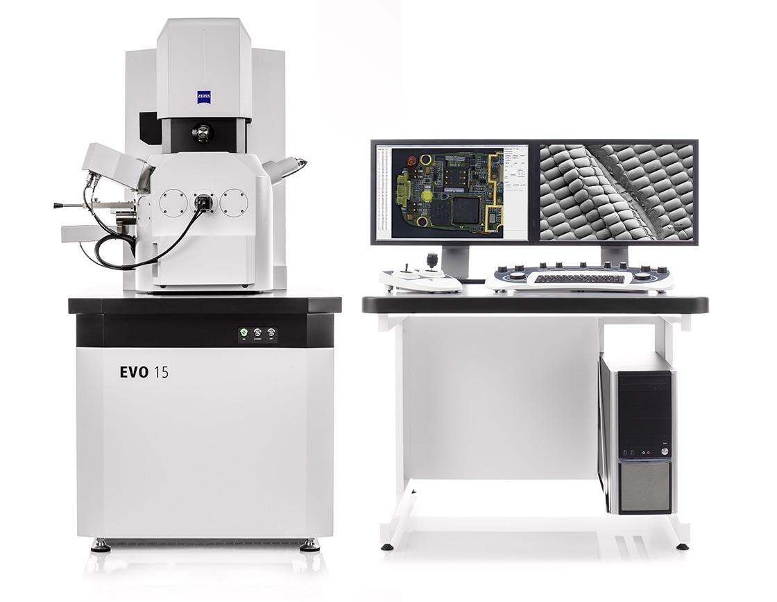
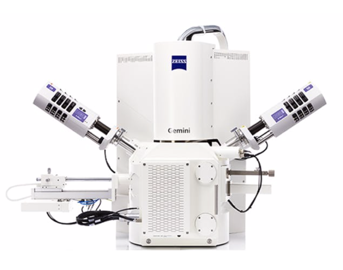
Any system can be configured with an ability to handle all materials, including non-conductive samples. Which SEM emitter is appropriate is dependent on the application. The below Zeiss SEM product line can address any and all applications and excel in the area of ease of use and performance.


